-
Notifications
You must be signed in to change notification settings - Fork 248
Learning Circuit
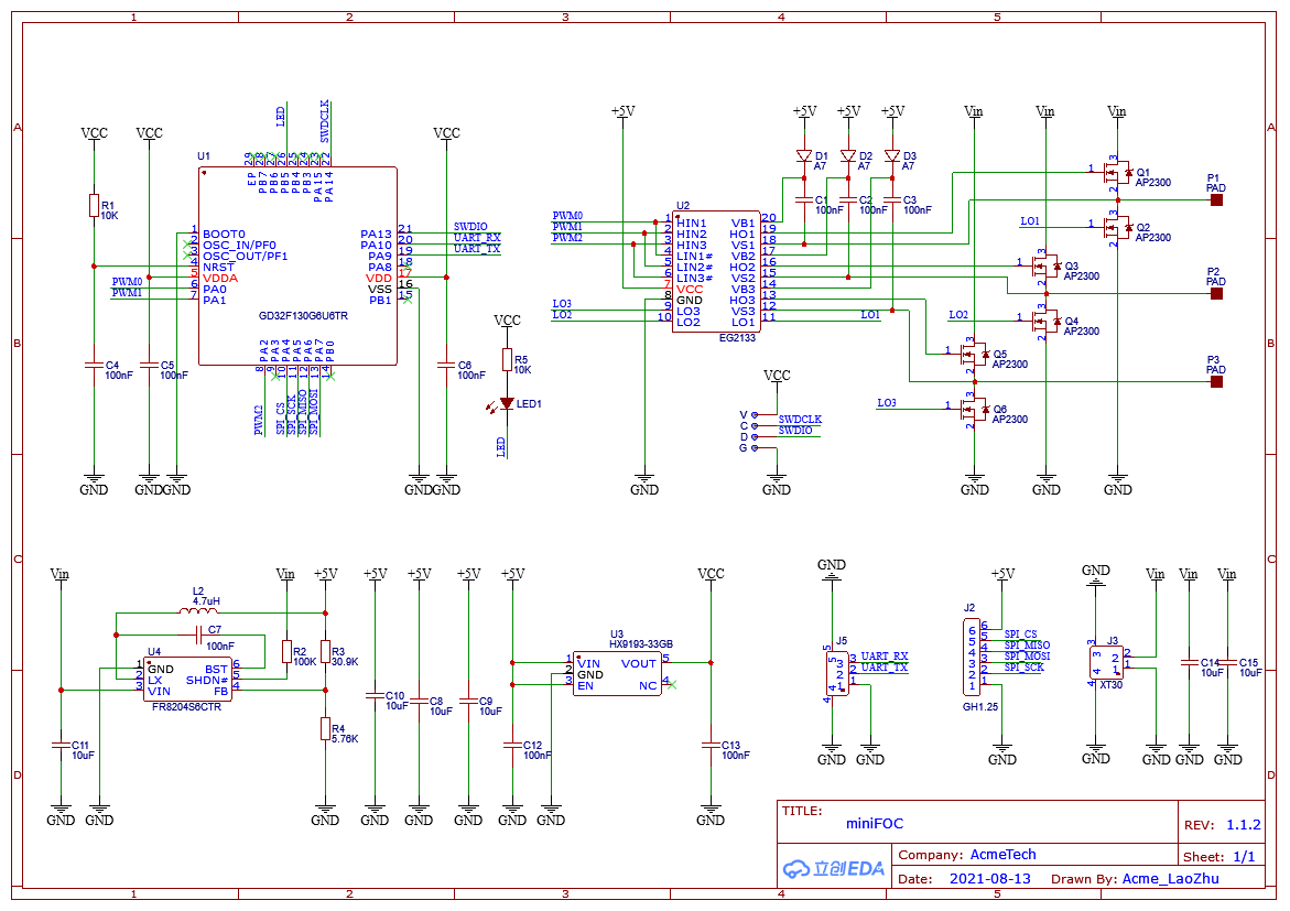
The following figure shows the schematic diagram of miniFOC demonstration circuit. Next, the circuit schematic diagram will be explained in the next step.

The main control of the demonstration circuit of miniFOC adopts the GD32F130G6U6 chip of GigaDevice. GD32F130G6U6 adopts ARM Cortex-M3 core, has 32KB flash space and 4KB SRAM space, and works at 72MHz frequency. PWM signals are generated through Timer1 channels 0, 1 and 2 (located at PA0, 1 and 2) of GD32 for driving the circuit. In addition, we also introduced UART0 and SWD debugging pins for program download and debugging. The magnetic encoder adopts SC60228 chip of Semiment, and the main control communicates with it through SPI0 interface.
EG2133 chip of EGmicro is selected for three-phase drive. EG2133 is a special three-phase independent half bridge driver chip, which has the advantages of 4.5-20v wide voltage input, 300V high side bootstrap power withstand voltage and so on. It can meet most circuit driving requirements, that is, there is no need to replace the driver IC and modify the program when replacing the MOSFET. The MOSFET of the demonstration circuit adopts AP2300 of All Power, with a drain source voltage of 20V and a drain current of 5.2A, which can meet the application requirements of general brushless motor. Since the maximum input voltage of the demonstration circuit is 18V, a two-stage step-down scheme is selected for the main control, grid drive and other peripheral power supplies. We selected Fitipower FR8204 chip as the first step-down to reduce the input voltage to 5V. FR8204 is a synchronous buck chip with integrated MOS. The input voltage range is 4.5-18v, the output current is 2a and the switching frequency is 500KHz, which provides a basis for circuit miniaturization. HX9193-33GB chip of HX is selected as the second step-down to provide 3.3V power supply for single chip microcomputer. Hx9193 is an LDO chip with an output current of 600mA.
The three-phase half bridge drive used in this design is EG2133 of EGmicro, the maximum PWM frequency that can be supported is 500KHz, and the hardware dead band control is built in, so the control part can ignore the setting of dead band, reduce the calculation resource consumption of microcontroller, and the withstand voltage of switch node is up to 275V. When applied to heavy load scenarios, it can also ensure that the half bridge drive is not damaged. There are 6 inputs on the three-phase half bridge drive, which can operate the six MOSFET separately, or directly connect the two inputs of a phase to the same PWM output port of the microcontroller, so that the half bridge maintains the complementary switch between the upper and lower MOSFET, which is different from using the 6 and 3 PWM output ports on the microcontroller, which are called 6PWM mode and 3PWM mode respectively.
PWM is generated by the general timer TIM1 peripheral in the GD32F130G6U6 microcontroller. In order to reduce the number of pins of the microcontroller, we use 3PWM mode for control, and the control signal of the lower MOSFET is driven by the complementary PWM generated by the three-phase driver.